FEFD
- orphan:
Directional Coupler
from pyOptiShared.DeviceGeometry import DeviceGeometry
from pyOptiShared.LayerInfo import LayerStack
from pyOptiShared.Material import ConstMaterial
import matplotlib.pyplot as plt
from FEMFy.FEFDSolver import FEFDSolver
from pyOptiShared.Simulator import PML_Params,Mesh
import numpy as np
import gdstk
filename = "DirectionalCoupler2.5.gds"
length = 11
width1 = 0.5
width2 = 0.5
gap = 0.15+0.25
lib = gdstk.Library()
shift=1.0
strt_wg = lib.new_cell("Straight_WG")
vertices1 = [(shift+0, -width1/2+gap), (shift+length, -width1/2+gap), (shift+length, width1/2+gap), (shift+0, width1/2+gap)]
vertices2 = [(0, -width2/2-gap), (length, -width2/2-gap), (length, width2/2-gap), (0, width2/2-gap)]
strt_wg.add(gdstk.Polygon(vertices1, layer=1))
strt_wg.add(gdstk.Polygon(vertices2, layer=1))
lib.write_gds(filename)
# Define Materials
si02_mat = ConstMaterial(mat_name="SiO2", epsReal=1.45**2,color='lightgreen')
sin_mat = ConstMaterial(mat_name="SiN", epsReal=1.99**2,color='lightblue')
# Creates the Layer Stack
layer_stack = LayerStack()
layer_stack.AddLayer(name="L1", number=1, thickness=0.22, zmin=0.0,
material=sin_mat, cladding=si02_mat)
layer_stack.SetBGandSub(background=si02_mat, substrate=si02_mat)
# Defines the Device Geometry
device_geometry = DeviceGeometry()
device_geometry.SetFromGDS(
layer_stack=layer_stack,
gds_file=filename,
buffers={'x':1.0,'y':2.0,'z':1.0}
)
device_geometry.SetAutoPortSettings(direction='x',port_buffer=2,pad=True)
# General Simulation Settings and Simulation Run
lmin = 1.5
lmax = 1.6
lcen = (lmax+lmin)/2
##########################################
### Mesh Settings ###
##########################################
fem_mesh=Mesh(dx=0.02,dy=0.02,dz=0.02)
fem_mesh.SetMeshOptions(mode='quiet',gui=False,export=True)
##########################################
### FEFDSolver Settings ###
##########################################
fefd_solver = FEFDSolver()
pml=PML_Params()
fefd_solver.SetBoundaries( min_x = "pml",
max_x = "pml",
min_y = "pml",
max_y = "pml",params=pml)
lams=np.linspace(start=1.5,stop=1.6,num=5)
fefd_solver.SetExcitation(wavelength=lams,
reciprocity='1x1')
fefd_solver.SetSimSettings(device_geometry = device_geometry,
mesh=fem_mesh,
wavelength=lams,
stability = 1.0,
resolution = 800,
interpolation = "FEM",
method = 'direct',
polarization='TM2.5',
number_iterations=2,
results_path='',
)
fefd_results = fefd_solver.Run()
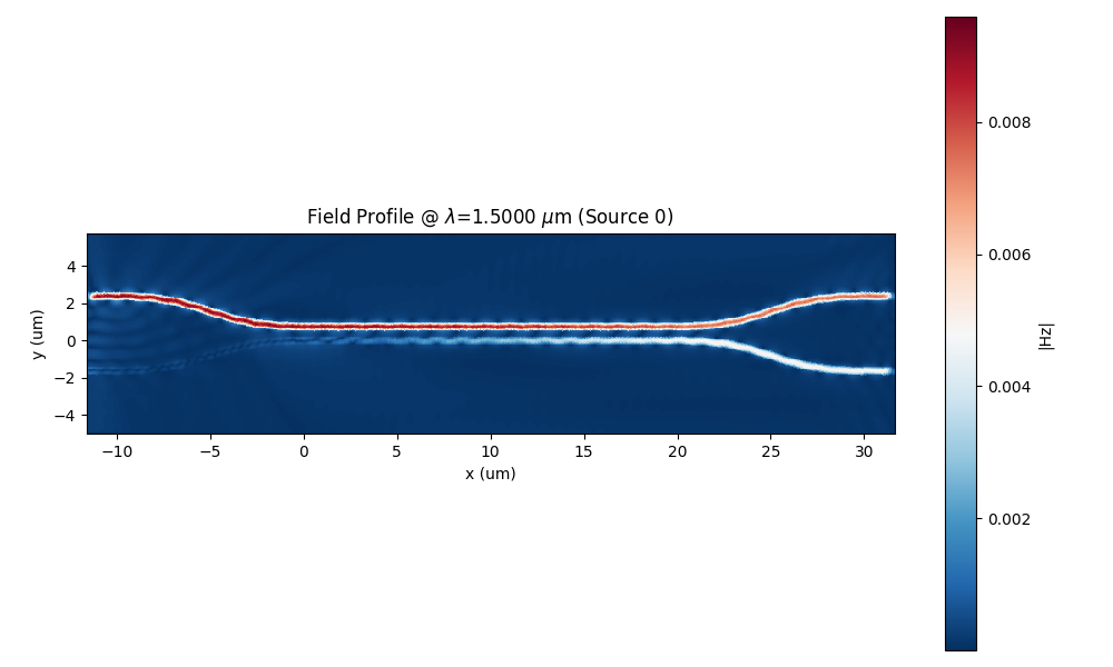
fefd_results.PlotField()
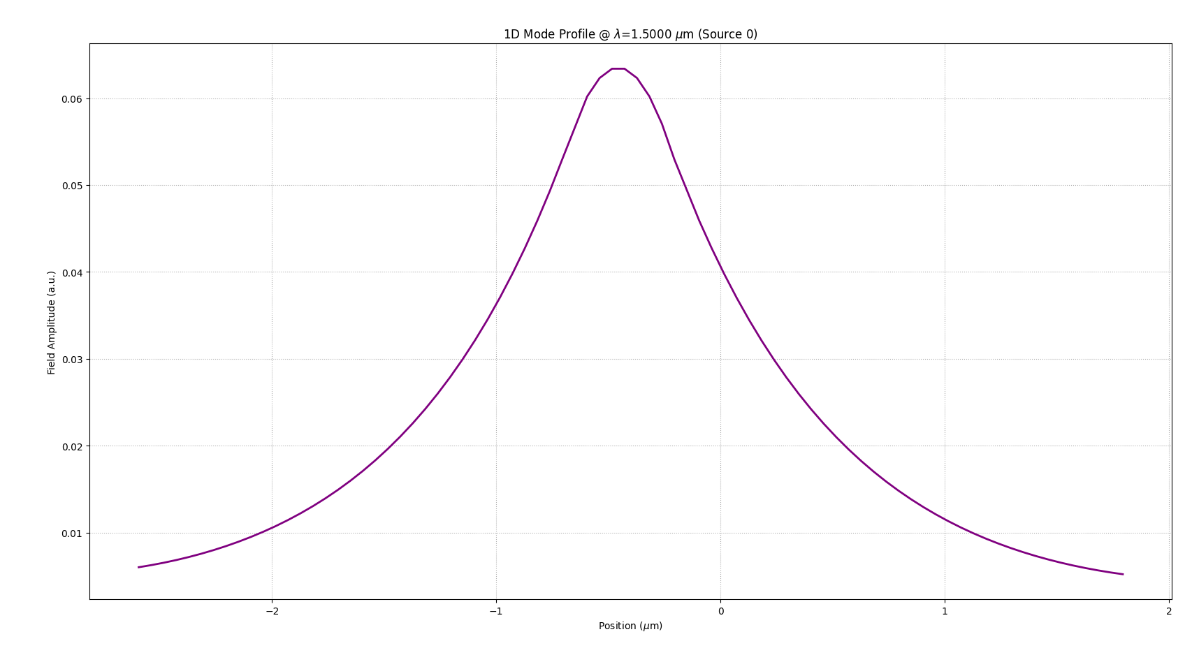
fefd_results.PlotPort()
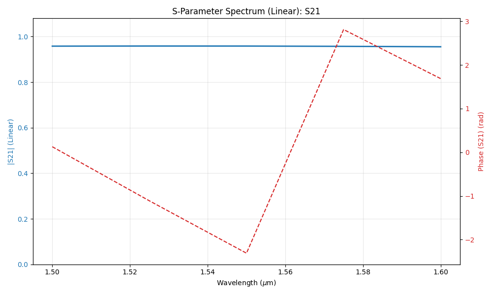
fefd_results.PlotSParameters(s_param="S21")
- orphan:
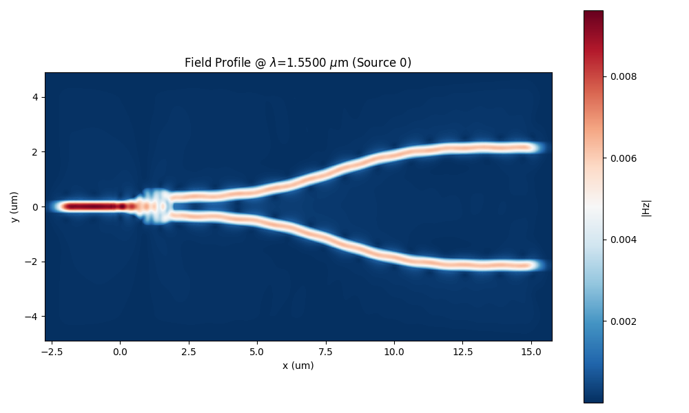
Splitter
For this example we are going to simulate a splitter (splitter.gds) and
then create an image with a DFT monitored field overlapping with the device structure outline.

In this particular example we make use of the DFT Monitor to monitor the frequency content of the fields, so we can plot a particular component and wavelength over the device structure outline. The python script for this simulation is presented in the following code snippet:
from pyOptiShared.DeviceGeometry import DeviceGeometry
from pyOptiShared.LayerInfo import LayerStack
from pyOptiShared.Material import ConstMaterial
from FEMFy.FEFDSolver import FEFDSolver
from pyOptiShared.Simulator import PML_Params, Mesh
import matplotlib.pyplot as plt
import numpy as np
# ==========================================
# 1. Material Definitions
# ==========================================
# Define materials needed for the simulation.
si02_mat = ConstMaterial(mat_name="SiO2", epsReal=1.45**2, color='lightgreen')
si_mat = ConstMaterial(mat_name="Si", epsReal=3.5**2, color='lightblue')
air_mat = ConstMaterial(mat_name="Air", epsReal=1**2, color='lightyellow')
# ==========================================
# 2. Layer Stack Configuration
# ==========================================
# Define the vertical layer structure.
# Even when importing a GDS (which provides 2D shapes), we must map those shapes
# to physical layers with thickness and material properties here.
layer_stack = LayerStack()
layer_stack.AddLayer(name="L1", number=1, thickness=0.22, zmin=0.0,
material=si_mat, cladding=si02_mat,
sideWallAng=0)
# Set background and substrate materials.
layer_stack.SetBGandSub(background=si02_mat, substrate=si02_mat)
# ==========================================
# 3. Device Geometry Setup (GDS Import)
# ==========================================
# Initialize the device geometry object.
device_geometry = DeviceGeometry()
# Instead of using 'SetFromFun', we use 'SetFromGDS' to load an external file.
# - gds_file: Path to the .gds file containing the design.
# - buffers: Padding around the GDS bounding box for the simulation region.
device_geometry.SetFromGDS(
layer_stack=layer_stack,
gds_file="splitter.gds",
buffers={'x': 2, 'y': 1.5, 'z': 1.5}
)
# ==========================================
# 4. Port Settings
# ==========================================
# Configure automatic port detection.
# 'reciprocity' in the solver settings often depends on how these ports are set up.
device_geometry.SetAutoPortSettings(direction='x', min=0, max=0.6, port_buffer=0.8, pad=False)
# ==========================================
# 5. Mesh Settings
# ==========================================
# Configure the finite element mesh size.
fem_mesh = Mesh(dx=0.08, dy=0.08, dz=0.04)
fem_mesh.SetMeshOptions(mode='quiet', gui=False, export=True)
# ==========================================
# 6. Solver Initialization & Boundaries
# ==========================================
fefd_solver = FEFDSolver()
# Initialize PML parameters (using defaults here as no specific args were passed).
pml = PML_Params()
# Apply boundaries to the solver instance.
fefd_solver.SetBoundaries(min_x="pml",
max_x="pml",
min_y="pml",
max_y="pml", params=pml)
# ==========================================
# 7. Excitation Settings
# ==========================================
# Define simulation wavelengths.
lams = np.linspace(start=1.5, stop=1.6, num=3)
# Set excitation parameters.
# 'reciprocity' is set to '1x2', which is typical for a 1-input, 2-output splitter,
# allowing the solver to optimize the simulation run.
fefd_solver.SetExcitation(wavelength=lams,
reciprocity='1x2')
# ==========================================
# 8. Final Solver Configuration
# ==========================================
# Pass all settings to the solver.
# Note the specific resolution, interpolation method, and polarization settings.
fefd_solver.SetSimSettings(
device_geometry=device_geometry,
mesh=fem_mesh,
wavelength=lams,
resolution=1000,
interpolation="cubic",
method='direct',
polarization='TM2.5',
number_iterations=2,
results_path='',
adjoint_info=None,
order=2
)
# ==========================================
# 9. Execution and Visualization
# ==========================================
# Run the simulation.
fefd_results = fefd_solver.Run()
# Visualize results.
# Plot the field specifically at 1.55um wavelength.
fefd_results.PlotField(target_wavelength=1.55)
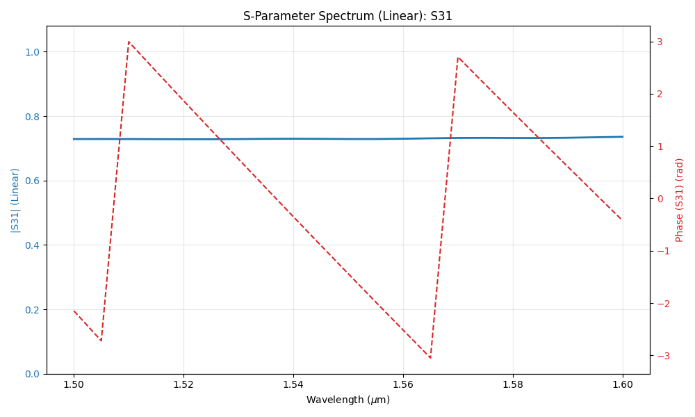
# Plot port locations and S-Parameters (specifically S31 transmission).
fefd_results.PlotPort()
fefd_results.PlotSParameters(s_param="S31")
- orphan:
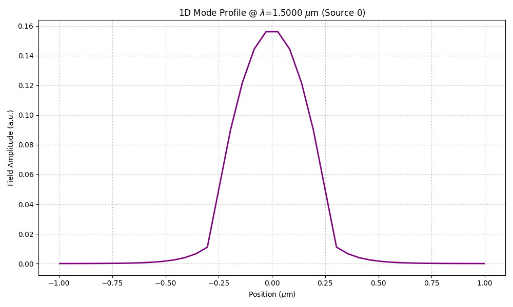
Waveguide - Run FEFD simulation from a function
Similarly for this example, we are going to simulate a straight waveguide from a user defined function.
from pyOptiShared.DeviceGeometry import DeviceGeometry
from pyOptiShared.LayerInfo import LayerStack
from pyOptiShared.Material import ConstMaterial,ExperimentalMaterial
from FEMFy.FEFDSolver import FEFDSolver
from pyOptiShared.Simulator import PML_Params, Mesh
import matplotlib.pyplot as plt
import numpy as np

# ==========================================
# 1. Material Definitions
# ==========================================
# Define materials needed for the simulation using the ConstMaterial class.
# We define the real permittivity (epsReal = n^2) and visualization colors.
si02_mat = ConstMaterial(mat_name="SiO2", epsReal=1.45**2, color='lightgreen')
si_mat = ConstMaterial(mat_name="Si", epsReal=3.5**2, color='lightblue')


# ==========================================
# 2. Layer Stack Configuration
# ==========================================
# Define the layer stack. We add layers based on the physical stackup.
# - 'material': The material of the geometry defined in this layer.
# - 'cladding': The material filling the rest of the layer outside the geometry.
layer_stack = LayerStack()
layer_stack.AddLayer(name="L1", number=1, thickness=0.22, zmin=0.0,
                     material=si_mat, cladding=si02_mat,
                     sideWallAng=0)

# Set the background (above stack) and substrate (below stack) materials.
layer_stack.SetBGandSub(background=si02_mat, substrate=si02_mat)


# ==========================================
# 3. Geometry Definition (Function-based)
# ==========================================
def waveguide(port_width=0.4, waveguide_length=5.00, input_port_center=(0, 0), layer=1):
    """
    Creates vertices for the structure to solve using polygons.

    Args:
        port_width: Width of the waveguide.
        waveguide_length: Length of the waveguide.
        input_port_center: Tuple (x, y) for the start position.
        layer: The layer number this geometry belongs to.

    Returns:
        A list of tuples in the format [(vertices, layer)].
    """
    vertices = [
        (input_port_center[0], input_port_center[1] - (port_width / 2)),
        (input_port_center[0] + waveguide_length, input_port_center[1] - (port_width / 2)),
        (input_port_center[0] + waveguide_length, input_port_center[1] + (port_width / 2)),
        (input_port_center[0], input_port_center[1] + (port_width / 2))
    ]

    return [(vertices, layer)]


# ==========================================
# 4. Parameter Definition
# ==========================================
# Define the parameters tuple to pass to the function during simulation.
# Format corresponds to function args: (port_width, waveguide_length, input_port_center, layer)
parameters = (0.4, 5.00, (0, 0), 1)


# ==========================================
# 5. Device Geometry Setup
# ==========================================
# Use DeviceGeometry to substitute parameters into the function and build the device.
# We also pass the layer stack and simulation region buffers (x, y, z).
device_geometry = DeviceGeometry()

device_geometry.SetFromFun(
    layer_stack=layer_stack,
    func=waveguide,
    parameters=parameters,
    buffers={'x': 1.5, 'y': 1.5, 'z': 1.5}
)


# ==========================================
# 6. Port Settings
# ==========================================
# Set automatic port detection based on direction (x or y) and buffer size.
device_geometry.SetAutoPortSettings(direction='x', port_buffer=1.3, pad=False)
device_geometry.PrintPorts()


# ==========================================
# 7. Simulation Parameters & PML
# ==========================================
# Define wavelength points (start, stop, number of points).
lams = np.linspace(start=1.5, stop=1.6, num=5)

# Set Perfectly Matched Layer (PML) parameters for the boundaries.
# This defines thickness, profile, kappa, sigma, and alpha for the absorbing layers.
pml = PML_Params()
# ==========================================
# 8. Mesh Settings
# ==========================================
# Configure the finite element mesh size (dx, dy, dz).
fem_mesh = Mesh(dx=0.02, dy=0.02)
fem_mesh.SetMeshOptions(mode='quiet', gui=False, export=True)


# ==========================================
# 9. Solver Initialization & Boundaries
# ==========================================
fefd_solver = FEFDSolver()

# Set boundaries for the solver (min/max x and y).
# We apply the PML parameters defined in step 7.
fefd_solver.SetBoundaries(min_x="pml",
                          max_x="pml",
                          min_y="pml",
                          max_y="pml",
                          params=pml)

# Set Excitation and Reciprocity.
# 'reciprocity' avoids simulating symmetrical ports unnecessarily.
fefd_solver.SetExcitation(wavelength=lams,
                          reciprocity='1x1')


# ==========================================
# 10. Final Solver Configuration
# ==========================================
# Pass all defined information (geometry, mesh, wavelength, solver settings) to the solver.
fefd_solver.SetSimSettings(
    device_geometry=device_geometry,
    mesh=fem_mesh,
    wavelength=lams,
    stability=1.0,
    resolution=200,
    interpolation="FEM",
    method='direct',
    polarization='TM2.5',
    number_iterations=2,
    order=2
)


# ==========================================
# 11. Execution and Visualization
# ==========================================
# Run the simulation.
results = fefd_solver.Run()

# Visualize the results: Fields, Ports, and S-Parameters.
results.PlotField()
results.PlotPort()
results.PlotSParameters(s_param="S21")
It is also possible to run sweeps on the function by using UpdateScriptParams which updates the parameters getting passed to the device geometry.
Note: you still need to call the solver SetSimSettings so that the device geometry update takes effect.
from pyOptiShared.DeviceGeometry import DeviceGeometry
from pyOptiShared.LayerInfo import LayerStack
from pyOptiShared.Material import ConstMaterial
from FEMFy.FEFDSolver import FEFDSolver
from pyOptiShared.Simulator import PML_Params, Mesh
import matplotlib.pyplot as plt
import numpy as np

# ==========================================
# 1. Material Definitions
# ==========================================
# Define materials needed for the simulation.
si02_mat = ConstMaterial(mat_name="SiO2", epsReal=1.45**2, color='lightgreen')
si_mat = ConstMaterial(mat_name="Si", epsReal=3.5**2, color='lightblue')
air_mat = ConstMaterial(mat_name="Air", epsReal=1**2, color='lightyellow')


# ==========================================
# 2. Layer Stack Configuration
# ==========================================
# Define the layer stack structure.
layer_stack = LayerStack()
layer_stack.AddLayer(name="L1", number=1, thickness=0.22, zmin=0.0,
                     material=si_mat, cladding=si02_mat,
                     sideWallAng=0)
layer_stack.SetBGandSub(background=si02_mat, substrate=si02_mat)


# ==========================================
# 3. Geometry Definition (Function-based)
# ==========================================
def waveguide(port_width=0.4, waveguide_length=1.00, input_port_center=(0, 0), layer=1):
    """
    Creates vertices for the waveguide structure.
    This function will be called repeatedly with updated parameters during the sweep.
    """
    vertices = [
        (input_port_center[0], input_port_center[1] - (port_width / 2)),
        (input_port_center[0] + waveguide_length, input_port_center[1] - (port_width / 2)),
        (input_port_center[0] + waveguide_length, input_port_center[1] + (port_width / 2)),
        (input_port_center[0], input_port_center[1] + (port_width / 2))
    ]
    return [(vertices, layer)]


# ==========================================
# 4. Sweep Parameter Setup
# ==========================================
# Define the range of widths to sweep over.
min_width = 0.3
max_width = 0.8
num_points = 3
widths = np.linspace(min_width, max_width, num_points)

# Define initial parameters tuple.
# Format: (port_width, waveguide_length, input_port_center, layer)
initial_parameters = (widths[0], 5.00, (0, 0), 1)


# ==========================================
# 5. Device Geometry Initialization
# ==========================================
# Initialize the device geometry with the function and INITIAL parameters.
# The parameters will be updated inside the loop later.
device_geometry = DeviceGeometry()

device_geometry.SetFromFun(
    layer_stack=layer_stack,
    func=waveguide,
    parameters=initial_parameters,
    buffers={'x': 1.5, 'y': 1.5, 'z': 1.5}
)

# Configure ports.
device_geometry.SetAutoPortSettings(direction='x', port_buffer=1,
                                    min=[0.1, 0.51], max=[0.55, 0.55], pad=False)


# ==========================================
# 6. Simulation Parameters
# ==========================================
# Wavelength points for the solver.
lams = np.linspace(start=1.5, stop=1.6, num=21)


# ==========================================
# 7. Mesh & PML Settings
# ==========================================
# Configure the mesh size.
fem_mesh = Mesh(dx=0.04, dy=0.04, dz=0.04)
fem_mesh.SetMeshOptions(mode='quiet', gui=False, export=True)

# Configure Perfectly Matched Layers (PML) for each boundary.
pml = PML_Params()
#pml.SetMinX(thickness=0.6, profile=2, kappa=1, sigma=1.3, alpha=0.00)
#pml.SetMaxX(thickness=0.6, profile=2, kappa=1, sigma=1.3, alpha=0.00)
#pml.SetMinY(thickness=0.1, profile=2, kappa=1, sigma=1.0, alpha=0.00)
#pml.SetMaxY(thickness=0.1, profile=2, kappa=1, sigma=1.0, alpha=0.00)

# ==========================================
# 8. Solver Initialization
# ==========================================
fefd_solver = FEFDSolver()

# Apply boundaries (PML) and excitation settings.
fefd_solver.SetBoundaries(min_x="pml",
                          max_x="pml",
                          min_y="pml",
                          max_y="pml", params=pml)

fefd_solver.SetExcitation(wavelength=lams,
                          reciprocity='1x1')


# ==========================================
# 9. Sweep Execution Loop
# ==========================================
# Iterate through each width in the defined array.
for w in widths:
    # 9a. Define filename for this specific iteration
    results_filename = 'waveguide_spx_1_50nm_sweep_' + str(w)
    print('solving for width : ', w)

    # 9b. Update Geometry Parameters
    # Create a new parameters tuple with the current width 'w'.
    # The other parameters (length, center, layer) remain constant.
    params = (w, 5.00, (0, 0), 1)

    # UpdateScriptParams applies the new parameters to the 'waveguide' function
    # defined in the DeviceGeometry object.
    device_geometry.UpdateScriptParams(params)


    # 9c. Update Solver Settings
    # Pass the updated device_geometry and unique filename to the solver.
    fefd_solver.SetSimSettings(
        device_geometry=device_geometry,
        mesh=fem_mesh,
        wavelength=lams,
        stability=1.0,
        resolution=500,
        interpolation="nearest",
        method='direct',
        polarization='TM2.5',
        number_iterations=2,
        order=2,
        device_name=results_filename,
    )

    # 9d. Run Simulation
    results = fefd_solver.Run()

    # 9e. Visualize Results
    # Plots will be generated for every iteration.
    results.PlotField(show=False)
    results.PlotPort(show=False)
    results.PlotSParameters(s_param="S21",show=False)
    print( f"width : {w} --- done !")
plt.show()

# Show all generated plots after the loop finishes.
Waveguide - Run FEFD simulation from a function (gdstk)
The function output can also be a gdstk library.
from pyOptiShared.DeviceGeometry import DeviceGeometry
from pyOptiShared.LayerInfo import LayerStack
from pyOptiShared.Material import ConstMaterial
from pyOptiShared.Designs import flex_taper
from FEMFy.FEFDSolver import FEFDSolver
from pyOptiShared.Simulator import PML_Params, Mesh
import matplotlib.pyplot as plt
import numpy as np

# ==========================================
# 1. Material Definitions
# ==========================================
# Define materials needed for the simulation.
si02_mat = ConstMaterial(mat_name="SiO2", epsReal=1.45**2, color='lightgreen')
si_mat = ConstMaterial(mat_name="Si", epsReal=3.5**2, color='lightblue')
air_mat = ConstMaterial(mat_name="Air", epsReal=1**2, color='lightyellow')


# ==========================================
# 2. Layer Stack Configuration
# ==========================================
# Define the layer stack.
# Note that even when using GDStk/Library functions, we must still assign
# the geometry to a specific layer number (here, layer 1) defined in this stack.
layer_stack = LayerStack()
layer_stack.AddLayer(name="L1", number=1, thickness=0.22, zmin=0.0,
                     material=si_mat, cladding=si02_mat,
                     sideWallAng=0)
layer_stack.SetBGandSub(background=si02_mat, substrate=si02_mat)


# ==========================================
# 3. Geometry Definition (Library Function)
# ==========================================
# Instead of defining a custom 'def waveguide(...)' function, we import
# 'flex_taper' from the 'pyOptiShared.Designs' library.
# This function uses GDStk internally to generate complex polygon structures.

# define the array of widths for the taper profile
widths = np.linspace(0.3, 1.0, 5)

# Define the parameters tuple required by 'flex_taper'.
# These likely correspond to: (width_array, length, width_start, width_end, etc., layer, boolean_flags)
parameters = (widths, 0.3, 1.0, 0.5, 2.0, 20, 1, False)


# ==========================================
# 4. Device Geometry Setup
# ==========================================
# Initialize the device geometry.
device_geometry = DeviceGeometry()

# Pass the imported 'flex_taper' function and its parameters.
# The 'SetFromFun' method handles the generation of vertices from the library function.
device_geometry.SetFromFun(
    layer_stack=layer_stack,
    func=flex_taper,
    parameters=parameters,
    buffers={'x': 1.5, 'y': 1.5, 'z': 1.5}
)

# Configure automatic port settings.
device_geometry.SetAutoPortSettings(direction='x', port_buffer=1,pad=False)


# ==========================================
# 5. Simulation Parameters
# ==========================================
# General simulation constants.

# Wavelength points for the solver.
lams = np.linspace(start=1.5, stop=1.6, num=5)


# ==========================================
# 6. Mesh & PML Settings
# ==========================================
# Configure the mesh size.
fem_mesh = Mesh(dx=0.01, dy=0.01, dz=0.01)
fem_mesh.SetMeshOptions(mode='quiet', gui=False, export=True)

# Configure Perfectly Matched Layers (PML) for boundaries.
pml = PML_Params()


# ==========================================
# 7. Solver Initialization
# ==========================================
fefd_solver = FEFDSolver()

# Apply boundaries (PML).
fefd_solver.SetBoundaries(min_x="pml",
                          max_x="pml",
                          min_y="pml",
                          max_y="pml", params=pml)

# Apply Excitation settings.
fefd_solver.SetExcitation(wavelength=lams,
                          reciprocity='1x1')


# ==========================================
# 8. Solver Configuration & Run
# ==========================================
# Pass all settings to the solver.
fefd_solver.SetSimSettings(order=2,
    device_geometry=device_geometry,
    mesh=fem_mesh,
    wavelength=lams,
    stability=1.0,
    resolution=400,
    interpolation="FEM",
    method='direct',
    polarization='TM2.5',
    number_iterations=2,
    device_name='flex_taper',
)

# Run the simulation.
results = fefd_solver.Run()

# ==========================================
# 9. Visualization
# ==========================================
results.PlotField()
results.PlotPort()
results.PlotSParameters(s_param="S21")