FEFD
API Documentation
Interface for running simulations in FEFD. |
|
Straight Waveguide
Through this example we will show the basic functions used to start simulating using FEM.
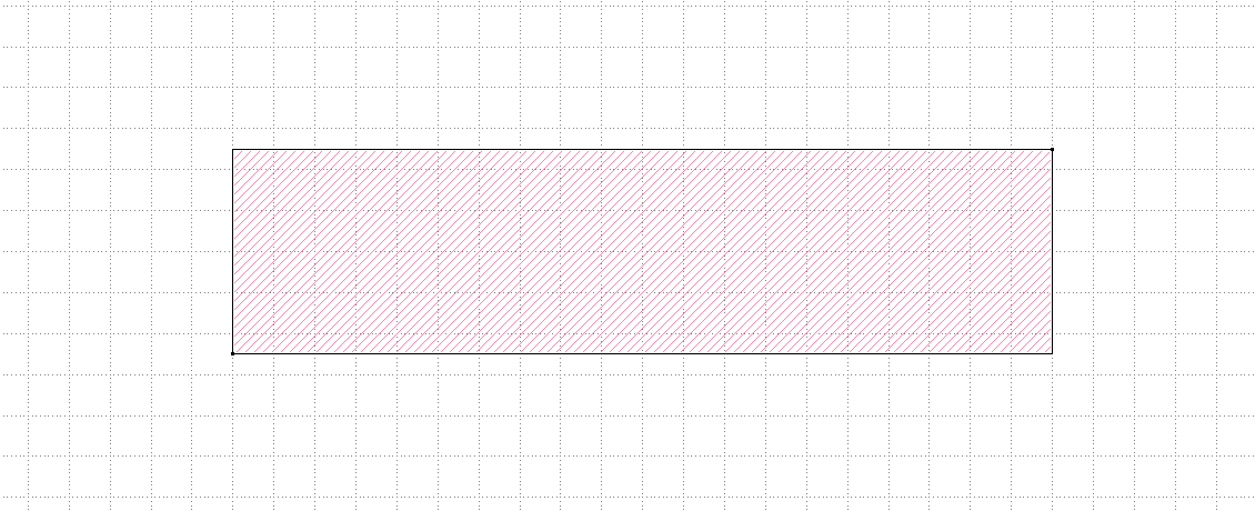
This examples simulates a straight waveguide (straightWG.gds):
The code used to simulate this waveguide is shown below.
"""Dielectric Waveguide Example running on FEMFy

"""
import numpy as np
from pyOptiShared.LayerInfo import LayerStack
from pyOptiShared.Material import ConstMaterial, SellmeierMaterial, ExperimentalMaterial
from pyOptiShared.DeviceGeometry import DeviceGeometry
from FEMFy.FEFDSolver import FEFDSolver
from pyOptiShared.Simulator import PML_Params,Mesh
import matplotlib.pyplot as plt

##########################################
###         Material Settings          ###
##########################################
myindex1p0 = ConstMaterial(mat_name="myindex1p0", epsReal=1.0**2)
myindex1p5 = ConstMaterial(mat_name="myindex3p5", epsReal=1.5**2)
mySellmeier = SellmeierMaterial(mat_name="mySellmeier", b_coeff=[1,2,3], c_coeff=[1,2,3])
myExperimental = ExperimentalMaterial(mat_name="myExperimental", lamb=[1,2,3], values=[1,2,3])

##########################################
###             Layer Stack            ###
##########################################
fem_mesh=Mesh(dx=0.02,dy=0.02,dz=0.02)
fem_mesh.SetMeshOptions(mode='quiet',gui=False,export=True)

layer_stack = LayerStack()
layer_stack.AddMaterial(mySellmeier)
layer_stack.AddMaterial(myExperimental)
layer_stack.AddLayer(name="L1", number=1, thickness=0.25, zmin=0.0,
                     material=myindex1p5, cladding=myindex1p0)
layer_stack.SetBGandSub(background=myindex1p0, substrate=myindex1p0)
### End Layer Stack


##########################################
###           Mesh Settings            ###
##########################################
fem_mesh=Mesh(dx=0.02,dy=0.02,dz=0.02)
fem_mesh.SetMeshOptions(mode='quiet',gui=False,export=True)
### End Mesh Settings

##########################################
###   Device Geometry/Port Settings    ###
##########################################

dvc_geometry = DeviceGeometry()
dvc_geometry.SetFromGDS(
    layer_stack=layer_stack,
    gds_file="straightWG.gds",
    buffers={'x':1.0,'y':1.5,'z':1.0},
)
dvc_geometry.SetAutoPortSettings(direction='x',min=0,max=0.6,port_buffer=1.0,pad=False)

### End Device Geometry

##########################################
###            PML Settings            ###
##########################################
pml=PML_Params()
pml.SetPMLParameters(thickness=[1.0,1.0,0.2,0.2],profile=3,kappa=1,sigma=[1.9,1.9,1.0,1.0],alpha=0.00)
### End PML Settings

##########################################
###       FEFDSolver Settings          ###
##########################################
fefd_solver = FEFDSolver()
fefd_solver.SetBoundaries(  min_x = "pml",
                            max_x = "pml",
                            min_y = "pml",
                            max_y = "pml",
                            params=pml)


lams=np.linspace(start=1.5,stop=1.6,num=3)

fefd_solver.SetExcitation(wavelength=lams,
                          reciprocity='1x1')

fefd_solver.SetSimSettings(device_geometry = dvc_geometry,
                           mesh=fem_mesh,
                           method = 'direct',
                           polarization='TM'
                           )
### End FEFDSolver Settings
##########################################
###         Run and Visualize          ###
##########################################
results = fefd_solver.Run()
results.PlotPort()
results.PlotField()
results.PlotNeff()
results.PlotSParameters(s_param="S21")
### End Visualize
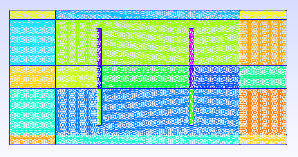
The class Mesh controls the parameters used for the FEM mesher, including visualizing and exporting an image of the mesh.
Gmesh GUI should pop up to show the mesh of the computational domain. It should look like this.
The class Pml_Params controls the parameters used for the FEM PML.
Dissimilar to a full 3D solver, FEM Frequency domain solver solves a 2D problem. Therefore, the two polarizations TE and TM become decoupled.
Therefore, in the SetSimSettings, the polarization has to be specified.
For this current development, the solver can handle TE, TM, TE2.5, and TM2.5.
The TE2.5 and TM2.5 take into account the thickness of the device by applying the variational in the depth direction.
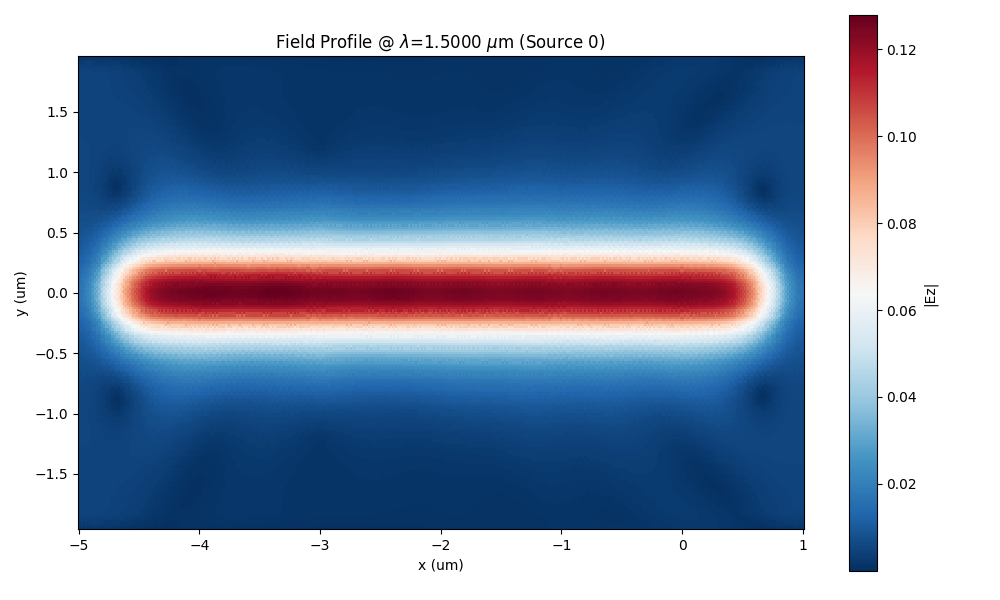
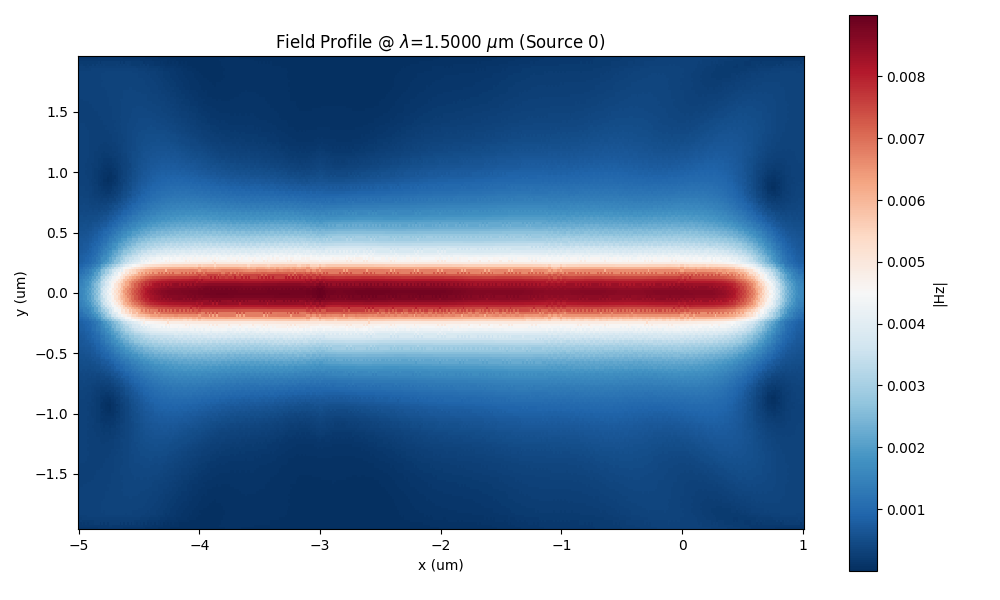
Field Profiles TE
For the TE solution, the field would look as shown below. The field would start decay efficiently in the PML as it can be observed. If the PML is not sufficiently suppressing the outgoing waves, ripples will appear inside the computational domain.
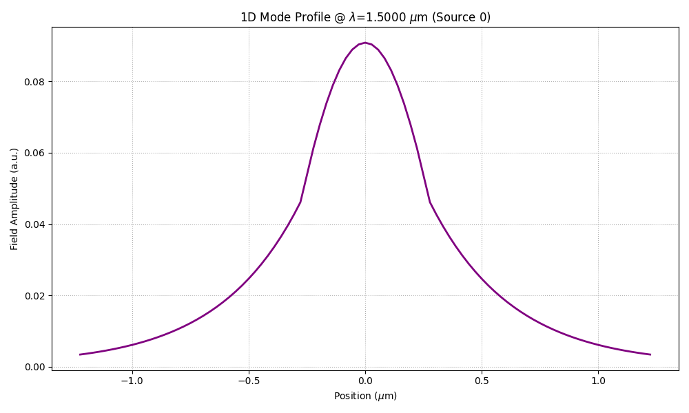
Port Profiles TE
For the TE solution, the mode profile of the TE solution should look continuous because of the continuity boundary conditions. For accurate results the port field should look decaying naturally with no ripples.

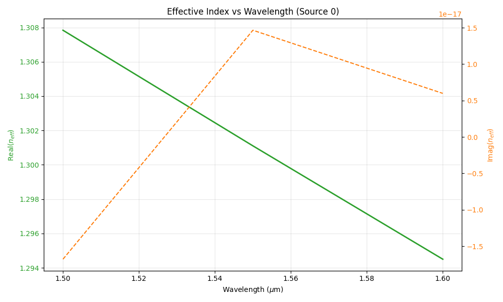
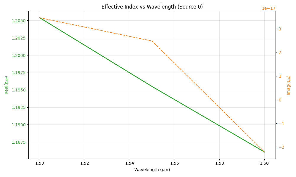
Port Effective Index TE
The corresponding effective index of the port mode vs wavelength should decrease with the increase of the wavelength as the profile gets more outside the core at longer wavelength.
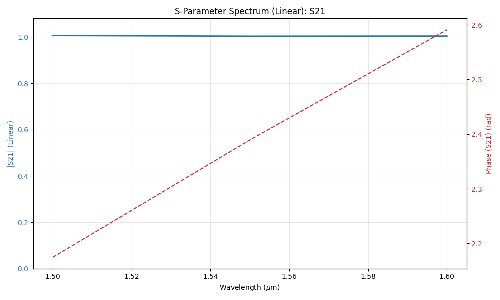
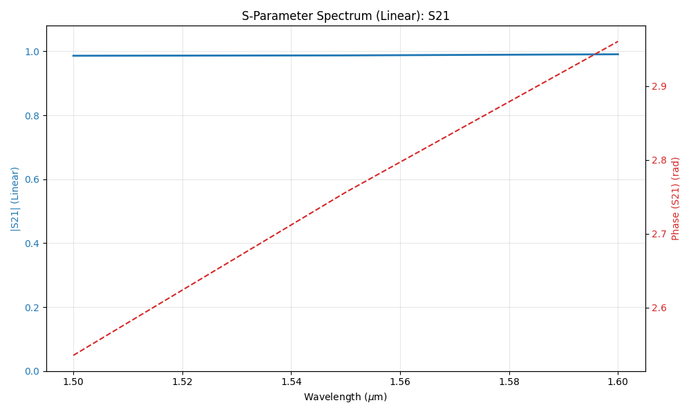
S21 Transmission TE
The transmission component of the S-parameter should indicate perfect transmission ~1. The phase should be a linear function in the wavelength.
Field Profiles TM
For the TM solution, the field would look as shown below. The field would start decay efficiently in the PML as it can be observed. If the PML is not sufficiently suppressing the outgoing waves, ripples will appear inside the computational domain.
Port Profiles TM
For the TM solution, the mode profile of the TM solution should look piece-wise continuous because of the discontinuity boundary conditions of the magnetic field derivative. For accurate results the port field should look decaying naturally with no ripples.
Port Effective Index TM
The corresponding effective index of the port mode vs wavelength should decrease with the increase of the wavelength as the profile gets more outside the core at longer wavelength.
S21 Transmission TM
The transmission component of the S-parameter should indicate perfect transmission ~1. The phase should be a linear function in the wavelength.
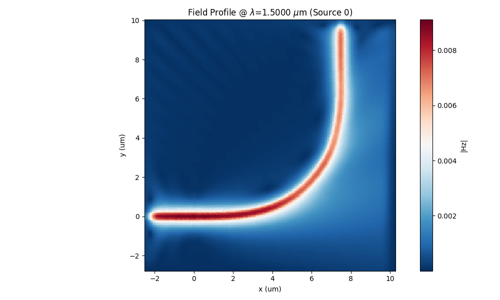
90 Degree Bend
This examples shows how the FEM handles curved structures (bend90.gds):

The simulation setup in the code snippet below. In this example, TM polarization is used
"""Dielectric Waveguide Example running on FEMFy

"""

import numpy as np
from pyOptiShared.LayerInfo import LayerStack
from pyOptiShared.Material import ConstMaterial, SellmeierMaterial, ExperimentalMaterial
from pyOptiShared.DeviceGeometry import DeviceGeometry
from pyOptiShared.DataStorage import ScatteredField2D
from FEMFy.FEFDSolver import FEFDSolver
from pyOptiShared.Simulator import PML_Params,Mesh
import matplotlib.pyplot as plt

##########################################
###         Material Settings          ###
##########################################
myindex1p00 = ConstMaterial(mat_name="myindex1p00", epsReal=1.0**2)
myindex1p5 = ConstMaterial(mat_name="myindex1p5", epsReal=1.5**2)
mySellmeier = SellmeierMaterial(mat_name="mySellmeier", b_coeff=[1,2,3], c_coeff=[1,2,3])
myExperimental = ExperimentalMaterial(mat_name="myExperimental", lamb=[1,2,3], values=[1,2,3])
##########################################
###           Mesh Settings            ###
##########################################
fem_mesh=Mesh(dx=0.02,dy=0.02)
fem_mesh.SetMeshOptions(mode='quiet',gui=False,export=True)


layer_stack = LayerStack()
layer_stack.AddMaterial(mySellmeier)
layer_stack.AddMaterial(myExperimental)
layer_stack.AddLayer(name="L1", number=1, thickness=0.25, zmin=0.0,
                     material=myindex1p5, cladding=myindex1p00)
layer_stack.SetBGandSub(background=myindex1p00, substrate=myindex1p00)

##########################################
###   Device Geometry/Port Settings    ###
##########################################

dvc_geometry = DeviceGeometry()
dvc_geometry.SetFromGDS(
    layer_stack=layer_stack,
    gds_file="bend90.gds",
    buffers={'x':2.5,'y':2.5,'z':1.0},
)
dvc_geometry.SetAutoPortSettings(direction='both',min=0.4,max=0.6,port_buffer=1.5,pad=False)
##########################################
###       FEFDSolver Settings          ###
##########################################
fefd_solver = FEFDSolver()

pml=PML_Params()


fefd_solver.SetBoundaries(  min_x = "pml",
                            max_x = "pml",
                            min_y = "pml",
                            max_y = "pml",
                            params=pml)


lams=np.linspace(start=1.5,stop=1.6,num=11)

fefd_solver.SetExcitation(wavelength=lams,
                          reciprocity='1x1')

fefd_solver.SetSimSettings(device_geometry = dvc_geometry,
                           mesh=fem_mesh,
                           method = 'direct',
                           polarization='TE',
                           resolution=800,
                           )

results = fefd_solver.Run()
results.PlotPort()
results.PlotField()
results.PlotNeff()
results.PlotSParameters(s_param="S21")
results.PlotSParameters(s_param="S11")
results.PlotMaterial()
#s21 = results.sparameters['S31'].Get('data')
#lam = results.sparameters['S31'].Get('wavelength')
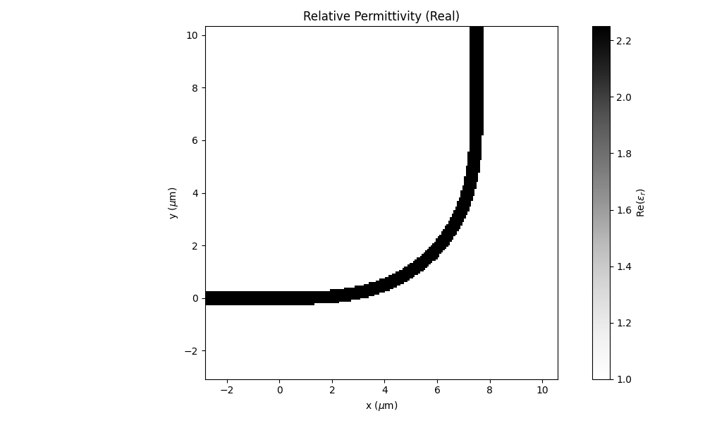
Permittivity profile
The relative permittivity profile would look like this. Note: the material distribution may look staggered just because of the interpolation of the scattered points for plotting. Using a high resolution for plotting would lessen this effect. You can control the resolution by changing resolution under the FEM solver settings
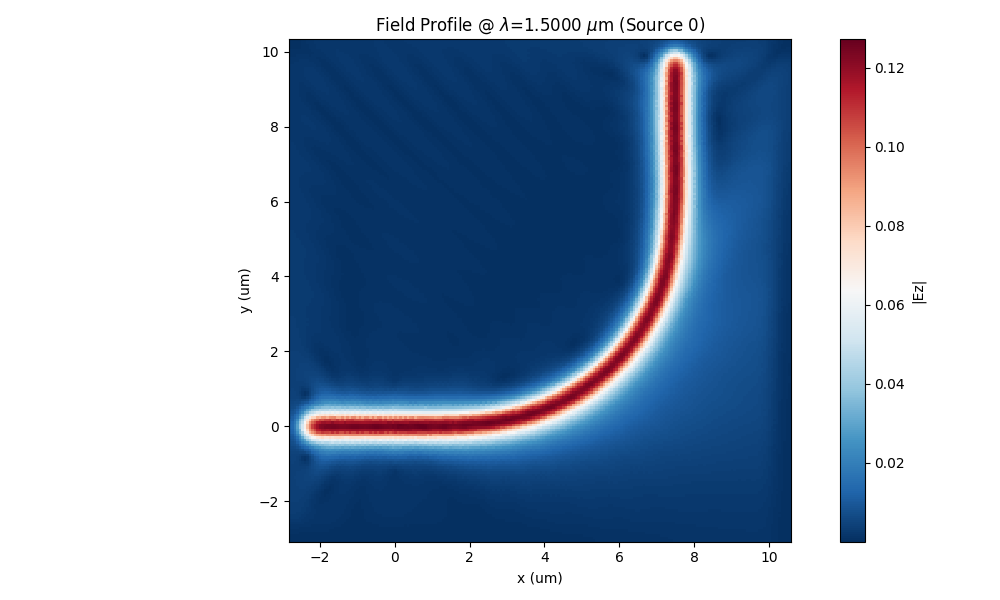
Field Profile TE
In the full field plots, the Ez field profile would look like this.
Port Profiles TE
For the TE solution, the mode profile of the TE solution should look continuous because of the continuity boundary conditions. For accurate results the port field should look decaying naturally with no ripples.
Port Effective Index TE
The corresponding effective index of the port mode vs wavelength should decrease with the increase of the wavelength as the profile gets more outside the core at longer wavelength.

S21 Transmission TE
The transmission component of the S-parameter should indicate perfect transmission ~1. The phase should be a linear function in the wavelength.
Field Profiles TM
For the TM solution, the field would look as shown below. The field would start decay efficiently in the PML as it can be observed. If the PML is not sufficiently suppressing the outgoing waves, ripples will appear inside the computational domain.
Port Profiles TM
For the TM solution, the mode profile of the TM solution should look piece-wise continuous because of the discontinuity boundary conditions of the magnetic field derivative. For accurate results the port field should look decaying naturally with no ripples.

Port Effective Index TM
The corresponding effective index of the port mode vs wavelength should decrease with the increase of the wavelength as the profile gets more outside the core at longer wavelength.

S21 Transmission TM
The transmission component of the S-parameter should indicate perfect transmission ~1. The phase should be a linear function in the wavelength.
2.5D simulation of Waveguide
This examples shows how to use FEM 2.5 D capabilities in simulating photonic devices and get results close to the 3D models. The example also shows how to simulate a device defined by a custom function
The simulation setup in the code snippet below. In this example, TM polarization is used.
from pyModeSolver.pyModeSolver import VFDModeSolver
from pyOptiShared.LayerInfo import LayerStack
from pyOptiShared.DeviceGeometry import DeviceGeometry
from pyOptiShared.Material import ConstMaterial
import gdstk
import numpy as np
import matplotlib.pyplot as plt
from matplotlib.patches import Polygon
from FEMFy.FEFDSolver import FEFDSolver
from pyOptiShared.Simulator import PML_Params,Mesh
from pyOptiShared.OptiShared import CalculateGroupIndex
##########################################
###             Waveguide function     ###
##########################################

def waveguide(port_width=0.4,waveguide_length=1.00,input_port_center=(0,0),layer=1):
    vertices=[(input_port_center[0],input_port_center[1]-(port_width/2)),
                (input_port_center[0]+waveguide_length,input_port_center[1]-(port_width/2)),
                (input_port_center[0]+waveguide_length,input_port_center[1]+(port_width/2)),
                (input_port_center[0],input_port_center[1]+(port_width/2))]

    return [(vertices,layer)]

##########################################
###         Material Settings          ###
##########################################
substrate_mat = ConstMaterial("SiO2", epsReal=1.44**2, epsImag=0.0)
core_mat = ConstMaterial("Si3N4", epsReal=1.99**2, epsImag=0.0)

##########################################
###       Layer Stack Settings         ###
##########################################
layer_stack = LayerStack()
layer_stack.AddLayer(number=1,material=core_mat, thickness=0.22, zmin=0, sideWallAng=0, cladding="Air_default")
layer_stack.SetBGandSub(background=substrate_mat, substrate=substrate_mat)


parameters=(0.5,2.00,(0,0),1) # (port_width,waveguide_length,input_port_center,layer)


##########################################
###      Visualize the waveguide       ###
##########################################

WG1=waveguide(*parameters)
vertices=WG1[0][0]

fig, ax = plt.subplots()
polygon = Polygon(vertices, closed=True, facecolor="lightcoral", edgecolor="black")
ax.add_patch(polygon)
plt.ylim([-1,1])
ax.set_xlabel('x [um]')
ax.set_ylabel('y [um]')
ax.set_title('Waveguide defined from function')


##########################################
###   Device Geometry/Port Settings    ###
##########################################
device_geometry = DeviceGeometry()
device_geometry.SetFromFun(layer_stack=layer_stack,
                           func=waveguide,
                           parameters=parameters,
                           buffers={'x':1.5,'y':4,'z':1.5})


device_geometry.SetAutoPortSettings(direction='x',min=0,max=0.6,port_buffer=3.0,pad=False)


##########################################
###       ModeSolver Settings          ###
##########################################
mode_solver = VFDModeSolver()
mode_solver.SetBoundaries(min_x = "pmc", max_x = "pmc",
                        min_y = "pmc", max_y = "pmc")

lams=np.linspace(start=1.5,stop=1.6,num=3)

mode_solver.SetSimSettings(device_geometry = device_geometry,
                           mesh={"dx": 0.02,"dy": 0.02, "dz": 0.02},
                           wavelength=lams,
                           nguess = 2.1,
                           nmodes = 1,
                           cut_plane = "YZ",
                           cut_location = 0.0,
                           tol = 1e-8,
                           results_path = "./ModeResults",
                           device_name = "my_results")

##########################################
###   Run and Results Visualization    ###
##########################################
mvd_results = mode_solver.Run()
print(mvd_results.Polarity(1.5))

#mvd_results.PlotMode(field='Hy') # Fundamental Mode Profile

Neff=mvd_results.neff.Get('neff')[0]
lam=mvd_results.neff.Get('wavelength')
#data=np.column_stack((lam,Neff))
#print(data)

##########################################
###           Mesh Settings            ###
##########################################
fem_mesh=Mesh(dx=0.02,dy=0.02,dz=0.02)
fem_mesh.SetMeshOptions(mode='quiet',gui=False,export=True)


##########################################
###       FEFDSolver Settings          ###
##########################################
fefd_solver = FEFDSolver()

pml=PML_Params()
pml.SetPMLParameters(thickness=[1.8,1.8,0.5,0.5],profile=2,kappa=1,sigma=[2,2,1.5,1.5],alpha=0.00)


fefd_solver.SetBoundaries(  min_x = "pml",
                            max_x = "pml",
                            min_y = "pml",
                            max_y = "pml",
                            params=pml)


fefd_solver.SetExcitation(wavelength=lams,
                          reciprocity='1x1')

fefd_solver.SetSimSettings(device_geometry = device_geometry,
                           mesh=fem_mesh,
                           method = 'direct',
                           polarization='TE2.5',
                           number_iterations=2
                           )

fefd_results = fefd_solver.Run()
fefd_results.PlotField()
#fefd_results.PlotNeff()
fem_lam=fefd_results.GetNeffData()[0]
fem_neff=fefd_results.GetNeffData()[1]
VFD_ng=CalculateGroupIndex(lam,np.real(Neff))
FEM_ng=CalculateGroupIndex(fem_lam,np.real(fem_neff))
fefd_results.PlotPort()
fefd_results.PlotSParameters(s_param="S21")
plt.figure()
plt.plot(fem_lam,np.real(fem_neff),label='FEM')
plt.plot(fem_lam,np.real(Neff),label='VFD')
plt.ylim([1,1.5])
plt.legend()
plt.xlabel('Wavelength [um]')
plt.ylabel('Index')
plt.show()
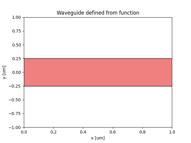
Waveguide plot
The code first starts by defining a waveguide from a function and plot it which looks like this
Then the code starts a mode solver instance to simulate the cross-section of the waveguide.
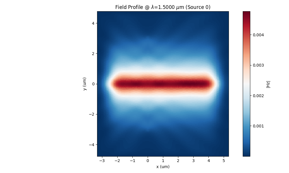
Field profile
The code should produce a field profile that looks like this
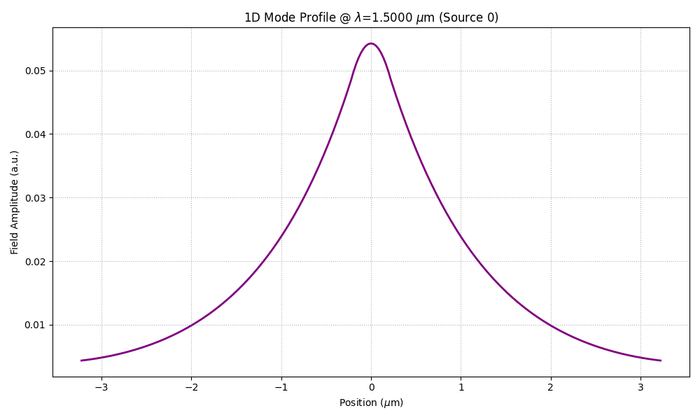
Field profile
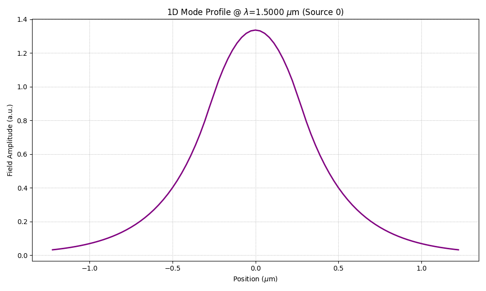
The code also plots the 1D field profile of the input port.
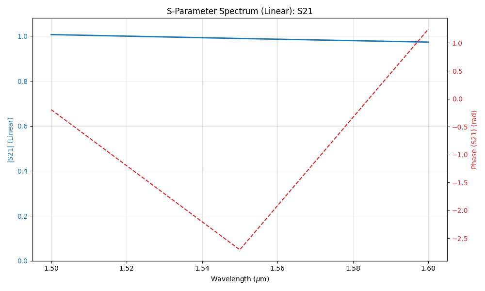
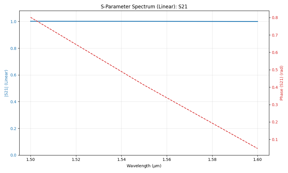
Transmission S21
The code also plots the S21 transmission parameter.
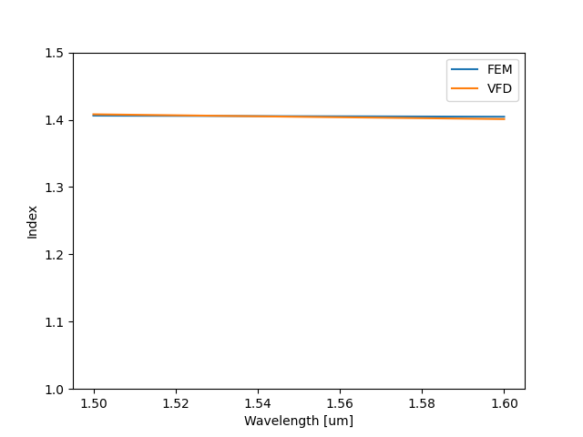
Effective index comparison
The code also plots a comparison between the effective index of the mode solver and the effective index computed with the 2.5D approximation.
2.5D simulation of Ring Resonator
This examples shows how to use FEM 2.5 D capabilities in simulating ring resonator and get results close to the 3D models. For this example we use a gds file.
The simulation setup in the code snippet below. In this example, TM polarization is used.
"""Dielectric Waveguide Example running on FEMFy

"""


import numpy as np
from pyOptiShared.LayerInfo import LayerStack
from pyOptiShared.Material import ConstMaterial, SellmeierMaterial, ExperimentalMaterial
from pyOptiShared.DeviceGeometry import DeviceGeometry
from FEMFy.FEFDSolver import FEFDSolver
from pyOptiShared.Simulator import PML_Params,Mesh
import matplotlib.pyplot as plt
from pyOptiShared.Utilities import loadsnpfile


##########################################
###         Material Settings          ###
##########################################
si02_mat = ConstMaterial(mat_name="SiO2", epsReal=1.45**2,color='lightgreen')
si_mat = ConstMaterial(mat_name="Si", epsReal=3.5**2,color='red')


# Creates the Layer Stack
layer_stack = LayerStack()
layer_stack.AddLayer(name="L1", number=1, thickness=0.22, zmin=0.0,
                    material=si_mat, cladding=si02_mat,
                    sideWallAng=0)
layer_stack.SetBGandSub(background=si02_mat, substrate=si02_mat)
##########################################
###   Device Geometry/Port Settings    ###
##########################################
port_center=[(0,0)]
port1_width=[0.5]
port2_width=[1.0]
taper_length=[10]
layer=[1]
init_params=(port_center,port1_width,port2_width,taper_length,layer)


dvc_geometry = DeviceGeometry()
dvc_geometry.SetFromGDS(
    layer_stack=layer_stack,
    gds_file="double_ring_100.gds",
    buffers={'x':1.0,'y':2,'z':1.0}
)
dvc_geometry.SetAutoPortSettings(direction='x',min=0,max=0.6,port_buffer=0.8,pad=False)
##########################################
###           Mesh Settings            ###
##########################################
fem_mesh=Mesh(dx=0.04,dy=0.04,dz=0.04)
fem_mesh.SetMeshOptions(mode='quiet',gui=False,export=True)
##########################################
###       FEFDSolver Settings          ###
##########################################
fefd_solver = FEFDSolver()

pml=PML_Params()
# pml.SetMinX(thickness=1.6,profile=2,kappa=1,sigma=1.6,alpha=0.00)
# pml.SetMaxX(thickness=1.6,profile=2,kappa=1,sigma=1.6,alpha=0.00)
# pml.SetMinY(thickness=0.1,profile=2,kappa=1,sigma=1.0,alpha=0.00)
# pml.SetMaxY(thickness=0.1,profile=2,kappa=1,sigma=1.0,alpha=0.00)

fefd_solver.SetBoundaries( min_x = "pml",
                            max_x = "pml",
                            min_y = "pml",
                            max_y = "pml",params=pml)


lams=np.linspace(start=1.547,stop=1.555,num=101)
fefd_solver.SetExcitation(wavelength=lams,
                          reciprocity='2x2')

fefd_solver.SetSimSettings(device_geometry = dvc_geometry,
                           mesh=fem_mesh,
                           wavelength=lams,
                           stability = 1,
                           resolution = 400,
                           interpolation = "cubic",
                           method = 'direct',
                           polarization='TM2.5',
                           number_iterations=2,
                           results_path='',
                           adjoint_info=None
                           )


fefd_results = fefd_solver.Run()
fefd_results.PlotField(target_wavelength=1.551)
fefd_results.PlotNeff()
fem_lam=fefd_results.GetNeffData()[0]
fem_neff=fefd_results.GetNeffData()[1]
s31=fefd_results.sparameters['S31'].Get('data')
lam=fefd_results.sparameters['S31'].Get('wavelength')
plt.figure()
plt.plot(lam,np.abs(s31),label='FEM |S31|')
plt.xlim([1.547,1.555])
plt.xlabel('Wavelength [um]')
fefd_results.PlotPort()
fefd_results.PlotSParameters(s_param="S31")
fefd_results.PlotSParameters(s_param="S21")
plt.show()
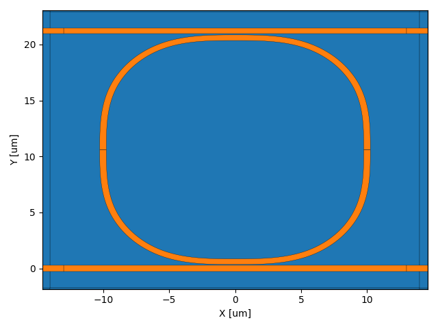
Ring Resonator plot
The code first starts by defining a waveguide from a function and plot it which looks like this
Then the code starts a mode solver instance to simulate the cross-section of the waveguide.
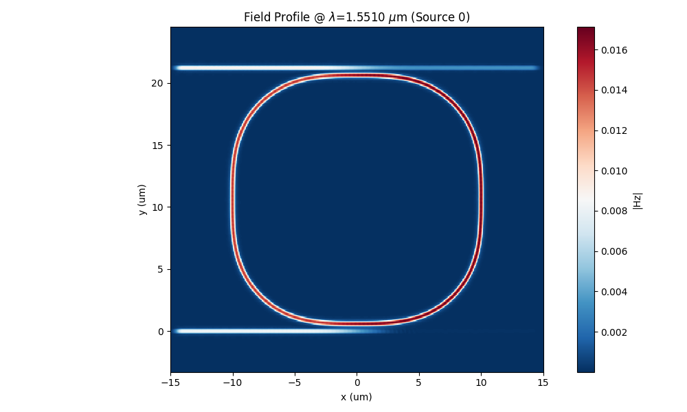
Field profile 1
The code should produce a field profile at the resonance frequency
Field profile 2
The code should produce a field profile outside the frequency

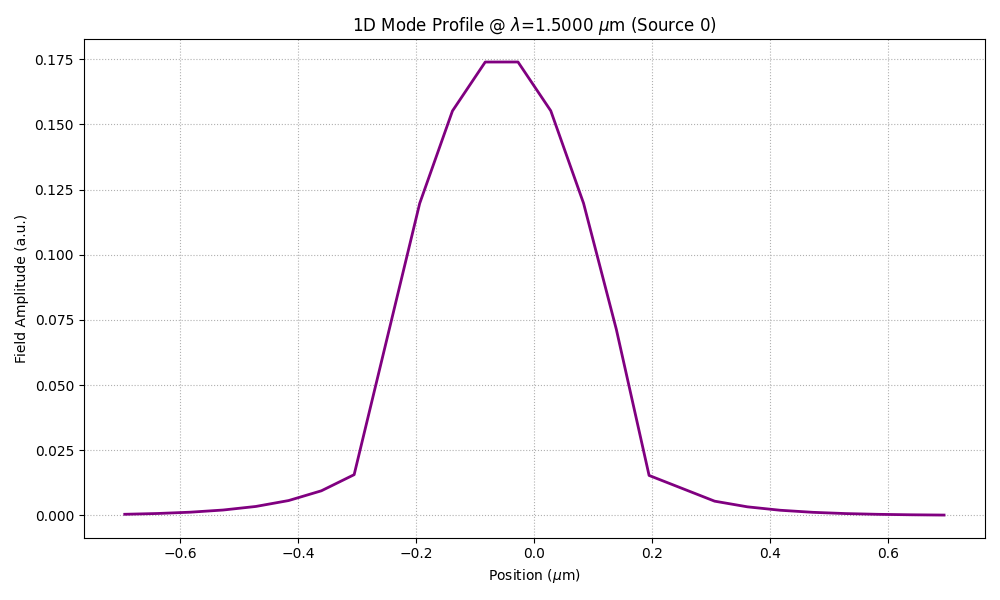
Port field
The code also plots the 1D field profile of the input port.
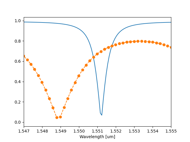
Transmission S31
The code also plots the S31 transmission parameter.
2.5D simulation of Directional Coupler
This examples shows how to use FEM 2.5 D capabilities in simulating directional coupler and get results close to the 3D models. For this example we use a gds file.
The simulation setup in the code snippet below. In this example, TM polarization is used.
from pyOptiShared.DeviceGeometry import DeviceGeometry
from pyOptiShared.LayerInfo import LayerStack
from pyOptiShared.Material import ConstMaterial
import matplotlib.pyplot as plt
from FEMFy.FEFDSolver import FEFDSolver
from pyOptiShared.Simulator import PML_Params,Mesh
from pyFDTDKernel.FDTDResults import FDTDResults
import numpy as np


filename = "coupler.gds"

# Define Materials
si02_mat = ConstMaterial(mat_name="SiO2", epsReal=1.45**2,color='lightgreen')
si_mat = ConstMaterial(mat_name="Si", epsReal=3.5**2,color='lightblue')

# Creates the Layer Stack
layer_stack = LayerStack()
layer_stack.AddLayer(name="L1", number=1, thickness=0.22, zmin=0.0,
                        material=si_mat, cladding=si02_mat)

layer_stack.SetBGandSub(background=si02_mat, substrate=si02_mat)

# Defines the Device Geometry
device_geometry = DeviceGeometry()
device_geometry.SetFromGDS(
    layer_stack=layer_stack,
    gds_file=filename,
    buffers={'x':1.0,'y':3.0,'z':1.0}
)
device_geometry.SetAutoPortSettings(direction='x',port_buffer=2,pad=False)

# General Simulation Settings and Simulation Run
lmin = 1.5
lmax = 1.6
lcen = (lmax+lmin)/2


##########################################
###           Mesh Settings            ###
##########################################
fem_mesh=Mesh(dx=0.04,dy=0.04,dz=0.04)
fem_mesh.SetMeshOptions(mode='quiet',gui=False,export=True)
##########################################
###       FEFDSolver Settings          ###
##########################################
fefd_solver = FEFDSolver()

pml=PML_Params()

fefd_solver.SetBoundaries( min_x = "pml",
                            max_x = "pml",
                            min_y = "pml",
                            max_y = "pml",params=pml)


lams=np.linspace(start=1.5,stop=1.6,num=25)
fefd_solver.SetExcitation(wavelength=lams,
                          reciprocity='2x2')

fefd_solver.SetSimSettings(device_geometry = device_geometry,
                           mesh=fem_mesh,
                           wavelength=lams,
                           resolution = 200,
                           interpolation = "nearest",
                           method = 'direct',
                           polarization='TM2.5',
                           number_iterations=2,
                           results_path='',
                           order=2
                           )


fefd_results = fefd_solver.Run()
fefd_results.PlotField()
fefd_results.PlotSParameters("S31")
fefd_results.PlotSParameters("S41")
fefd_results.PlotPort()


fefd_S31=fefd_results.sparameters['S31'].Get('data')

lam=fefd_results.sparameters['S31'].Get('wavelength')
fefd_S41=fefd_results.sparameters['S41'].Get('data')

plt.figure()
plt.plot(lam,abs(fefd_S31),'--o',label='Abs S31_FEFD')
plt.ylim([0.3,1])
plt.xlabel('wavelength [um]')
plt.legend()


plt.figure()
plt.plot(lam,abs(fefd_S41),'--o',label='Abs S41_FEFD')
plt.xlabel('wavelength [um]')
plt.ylim([0.3,1])
plt.legend()

plt.show()
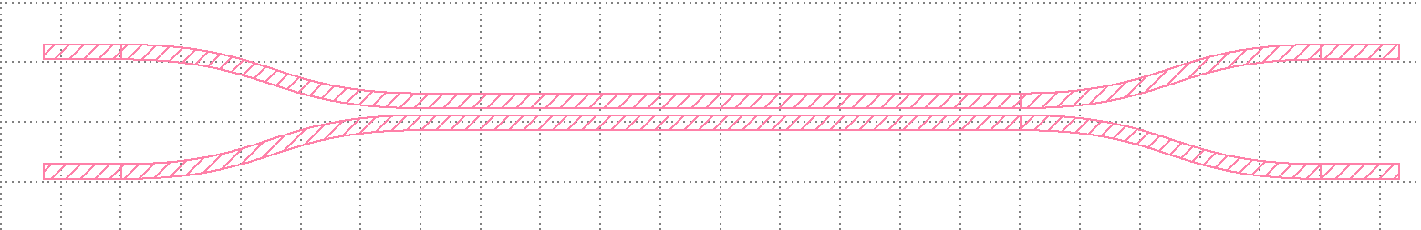
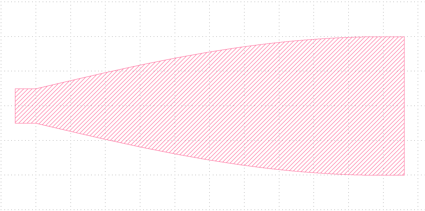
Directional Coupler plot
The code first starts by defining a waveguide from a gds and plot it which looks like this
Then the code starts a mode solver instance to simulate the cross-section of the waveguide.
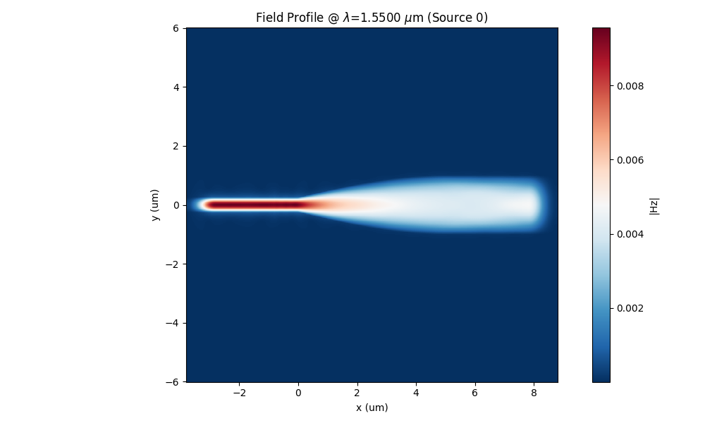
Field profile
The code should produce a field profile at 1.5 that looks like

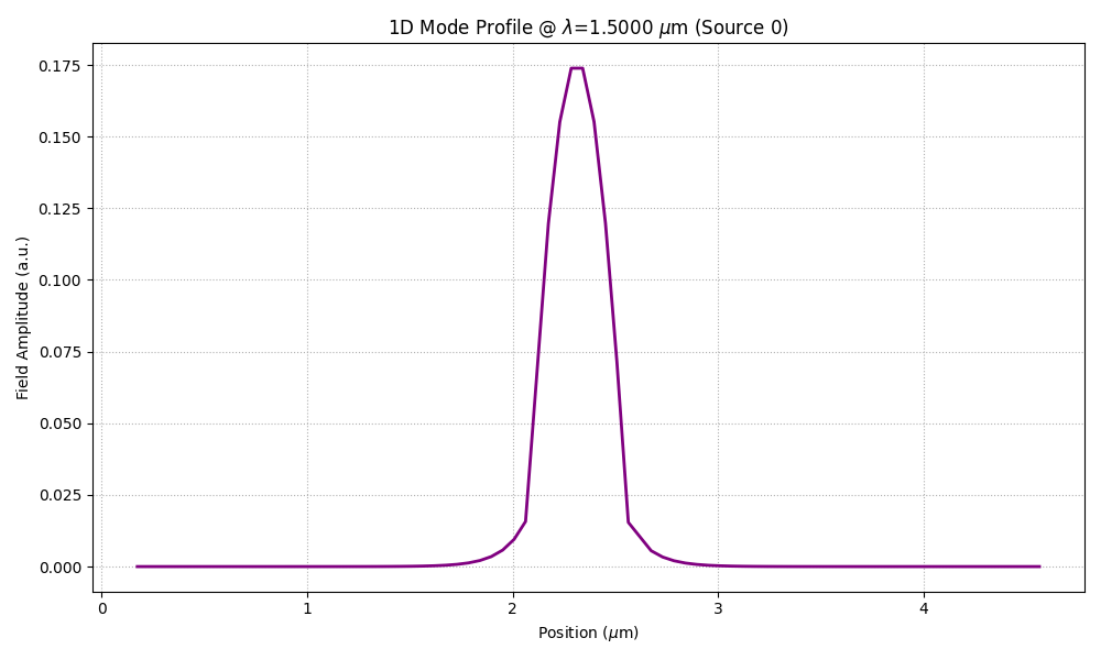
Port field
The code also plots the 1D field profile of the input port.
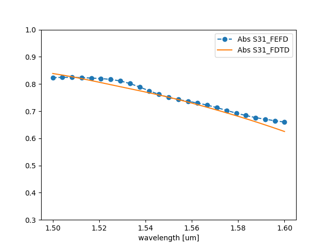
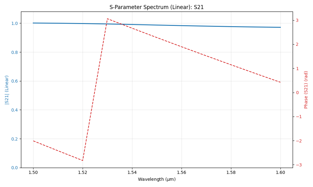
S31
The code also plots the S31 transmission parameter that compared with full 3D simulation should look like.
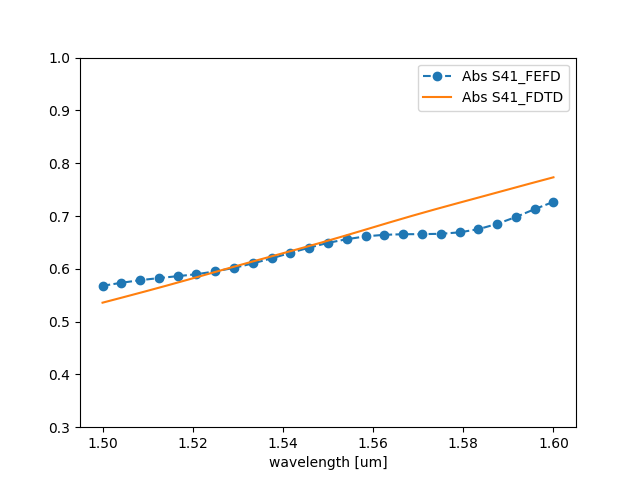
S41
The code also plots the S41 transmission parameter that compared with full 3D simulation should look like.
2.5D simulation of Cosine Taper
This examples shows how to use FEM 2.5 D capabilities in simulating Cosine Taper and get results close to the 3D models. For this example we use a gds file.
The simulation setup in the code snippet below. In this example, TM polarization is used.
from pyOptiShared.DeviceGeometry import DeviceGeometry
from pyOptiShared.LayerInfo import LayerStack
from pyOptiShared.Material import ConstMaterial
import matplotlib.pyplot as plt
from FEMFy.FEFDSolver import FEFDSolver
from pyOptiShared.Simulator import PML_Params,Mesh
from pyOptiShared.Designs import cosine_taper
import numpy as np

import gdstk
input_length:float=0.8
in_width:float=0.5
out_width:float=2
max_width:float=2
taper_length=5.00
resolution:int=40


taper_lib=cosine_taper(input_length,in_width,out_width,max_width,taper_length)

filename='cosine_taper.gds'
taper_lib.write_gds(filename)


# Define Materials
si02_mat = ConstMaterial(mat_name="SiO2", epsReal=1.45**2,color='lightgreen')
si_mat = ConstMaterial(mat_name="Si", epsReal=3.5**2,color='lightblue')

# Creates the Layer Stack
layer_stack = LayerStack()
layer_stack.AddLayer(name="L1", number=1, thickness=0.22, zmin=0.0,
                        material=si_mat, cladding=si02_mat)

layer_stack.SetBGandSub(background=si02_mat, substrate=si02_mat)

# Defines the Device Geometry
device_geometry = DeviceGeometry()
device_geometry.SetFromGDS(
    layer_stack=layer_stack,
    gds_file=filename,
    buffers={'x':2.0,'y':2.0,'z':1.0}
)
device_geometry.SetAutoPortSettings(direction='x',port_buffer=2.5,pad=False)

# General Simulation Settings and Simulation Run
lmin = 1.5
lmax = 1.6


##########################################
###           Mesh Settings            ###
##########################################
fem_mesh=Mesh(dx=0.02,dy=0.02,dz=0.02)
fem_mesh.SetMeshOptions(mode='quiet',gui=False,export=False)
##########################################
###       FEFDSolver Settings          ###
##########################################
fefd_solver = FEFDSolver()

pml=PML_Params()

fefd_solver.SetBoundaries( min_x = "pml",
                            max_x = "pml",
                            min_y = "pml",
                            max_y = "pml",params=pml)


lams=np.linspace(start=1.5,stop=1.6,num=21)
fefd_solver.SetExcitation(wavelength=lams,
                          reciprocity='1x1')

fefd_solver.SetSimSettings(device_geometry = device_geometry,
                           mesh=fem_mesh,
                           wavelength=lams,
                           resolution = 800,
                           interpolation = "FEM",
                           method = 'direct',
                           polarization='TM2.5',
                           number_iterations=2,
                           results_path='',
                           )


fefd_results = fefd_solver.Run()
fefd_results.PlotField(1.55)
fefd_results.PlotPort()
fefd_results.PlotSParameters(s_param="S21")
Cosine_Taper plot
The code first starts by defining a waveguide from a gds and plot it which looks like this
Then the code starts a mode solver instance to simulate the cross-section of the waveguide.
Field profile
The code should produce a field profile at 1.5 that looks like
Port field
The code also plots the 1D field profile of the input port.

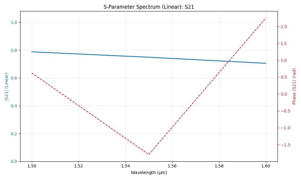
S21
The code also plots the S21 transmission parameter that compared with full 3D simulation should look like.
2.5D simulation of MMI 1x2
This examples shows how to use FEM 2.5 D capabilities in simulating MMI1x2 and get results close to the 3D models. For this example we use a gds file.
The simulation setup in the code snippet below. In this example, TM polarization is used.
from pyOptiShared.DeviceGeometry import DeviceGeometry
from pyOptiShared.LayerInfo import LayerStack
from pyOptiShared.Material import ConstMaterial
import matplotlib.pyplot as plt
from FEMFy.FEFDSolver import FEFDSolver
from pyOptiShared.Simulator import PML_Params, Mesh
from pyFDTDKernel.FDTDResults import FDTDResults
import numpy as np
import gdstk

# Define the filename for the GDS geometry
filename = "mmi1x2_with_sbend.gds"


# ==========================================
# 1. Material Definitions
# ==========================================
# Define materials needed for the simulation.
si02_mat = ConstMaterial(mat_name="SiO2", epsReal=1.45**2, color='lightgreen')
si_mat = ConstMaterial(mat_name="Si", epsReal=3.5**2, color='lightblue')


# ==========================================
# 2. Layer Stack Configuration
# ==========================================
# Define the layer stack.
layer_stack = LayerStack()
layer_stack.AddLayer(name="L1", number=1, thickness=0.22, zmin=0.0,
                     material=si_mat, cladding=si02_mat)

# Set background and substrate materials.
layer_stack.SetBGandSub(background=si02_mat, substrate=si02_mat)


# ==========================================
# 3. Device Geometry Setup (GDS Import)
# ==========================================
# Initialize device geometry and load from GDS file.
device_geometry = DeviceGeometry()
device_geometry.SetFromGDS(
    layer_stack=layer_stack,
    gds_file=filename,
    buffers={'x': 1.0, 'y': 4.0, 'z': 1.0}
)


# ==========================================
# 4. Port Settings
# ==========================================
# Configure automatic port detection.
device_geometry.SetAutoPortSettings(direction='x', port_buffer=2, max=1.3, min=0.1, pad=False)


# ==========================================
# 5. Mesh Settings
# ==========================================
# Configure the finite element mesh size.
fem_mesh = Mesh(dx=0.04, dy=0.04, dz=0.04)
fem_mesh.SetMeshOptions(mode='quiet', gui=False, export=True)


# ==========================================
# 6. PML & Boundary Conditions
# ==========================================
# Initialize solver and PML parameters.
fefd_solver = FEFDSolver()
pml = PML_Params()

# Set explicit PML parameters for Min/Max X and Y boundaries.


# Apply boundaries to the solver.
fefd_solver.SetBoundaries(min_x="pml",
                          max_x="pml",
                          min_y="pml",
                          max_y="pml", params=pml)


# ==========================================
# 7. Excitation Settings
# ==========================================
# Define wavelength sweep range.
lmin = 1.5
lmax = 1.6
lams = np.linspace(start=lmin, stop=lmax, num=5)

# Set excitation wavelengths and reciprocity.
fefd_solver.SetExcitation(wavelength=lams,
                          reciprocity='1x2')


# ==========================================
# 8. Solver Configuration & Execution
# ==========================================
# Pass all settings to the solver.
fefd_solver.SetSimSettings(
    device_geometry=device_geometry,
    order=2,
    mesh=fem_mesh,
    wavelength=lams,
    stability=1.0,
    resolution=1000,
    interpolation="FEM",
    method='direct',
    polarization='TM2.5',
    number_iterations=2,
    results_path='',
)

# Run the FEFD simulation.
fefd_results = fefd_solver.Run()

# Visualize immediate FEFD results.
fefd_results.PlotField()
fefd_results.PlotSParameters("S21")
fefd_results.PlotSParameters("S31")
fefd_results.PlotPort()


# ==========================================
# 9. Validation: Compare with FDTD Results
# ==========================================
# This section loads pre-calculated FDTD results to benchmark the FEFD solver.

# 9a. Load FDTD data from HDF5 file
fdtd_results = FDTDResults()
# Note: This path is specific to the local machine and points to a previous simulation result.
fdtd_results.loadHDF5(r'fdtd_mmi1x2.hdf5')

# 9b. Extract Data for Comparison
# Extract S21 and S31 parameters from the loaded FDTD results.
fdtd_S21 = fdtd_results.sparameters['S21'].Get('data')
fdtd_S31 = fdtd_results.sparameters['S31'].Get('data')
fdtd_lam = fdtd_results.sparameters['S21'].Get('wavelength')

# Extract S21 and S31 parameters from the current FEFD run.
fefd_S21 = fefd_results.sparameters['S21'].Get('data')
fefd_S31 = fefd_results.sparameters['S31'].Get('data')
lam = fefd_results.sparameters['S21'].Get('wavelength')


# 9c. Plot Comparison (S31)
plt.figure()
plt.plot(lam, abs(fefd_S31), '--o', label='Abs S31_FEFD')
plt.plot(fdtd_lam, abs(fdtd_S31), label='Abs S31_FDTD')
plt.ylim([0.2, 1])
plt.xlabel('wavelength [um]')
plt.legend()


# 9d. Plot Comparison (S21)
plt.figure()
plt.plot(lam, abs(fefd_S21), '--o', label='Abs S21_FEFD')
plt.plot(fdtd_lam, abs(fdtd_S21), label='Abs S21_FDTD')
plt.xlabel('wavelength [um]')
plt.ylim([0.2, 1])
plt.legend()
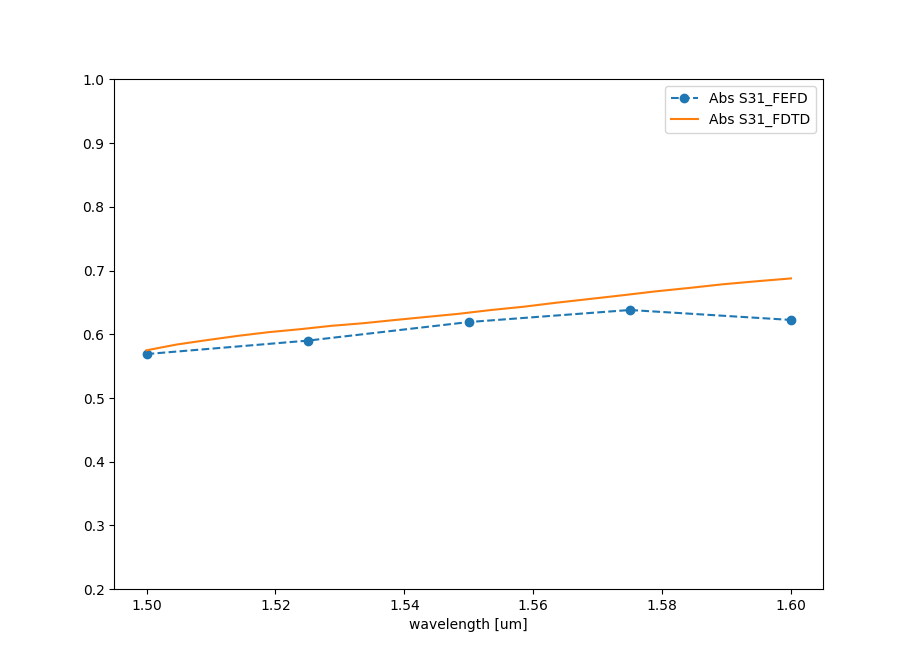
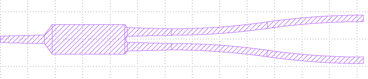
MMI1x2 plot
The code first starts by defining a waveguide from a gds and plot it which looks like this
Then the code starts a mode solver instance to simulate the cross-section of the waveguide.
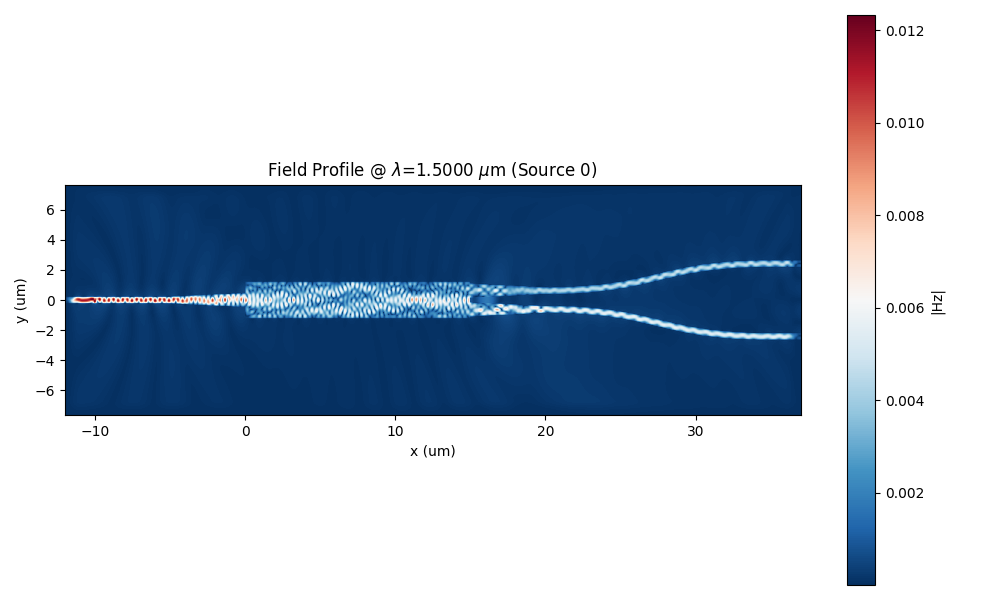
Field profile
The code should produce a field profile at 1.5 that looks like
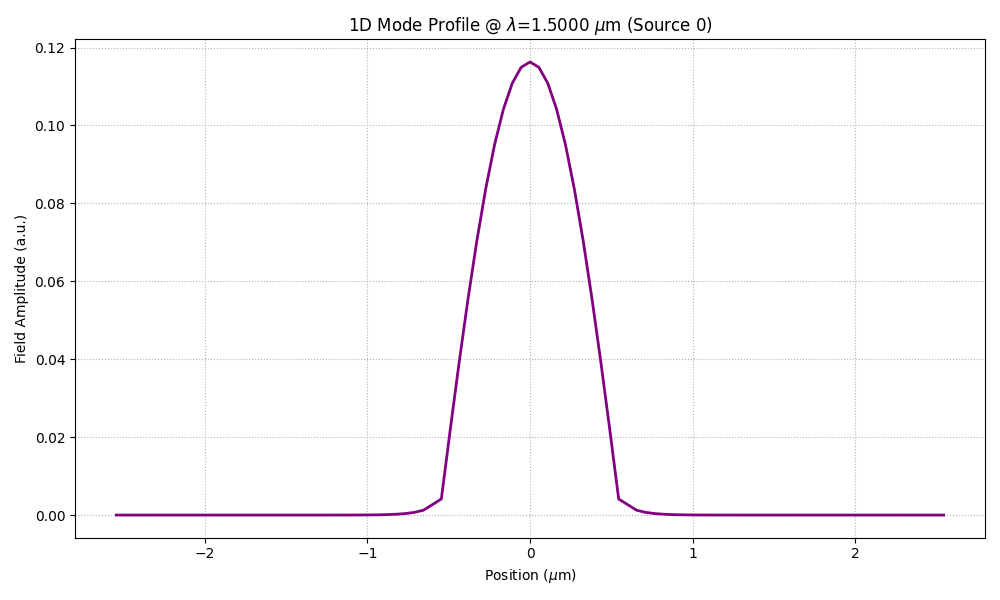
Port field
The code also plots the 1D field profile of the input port.
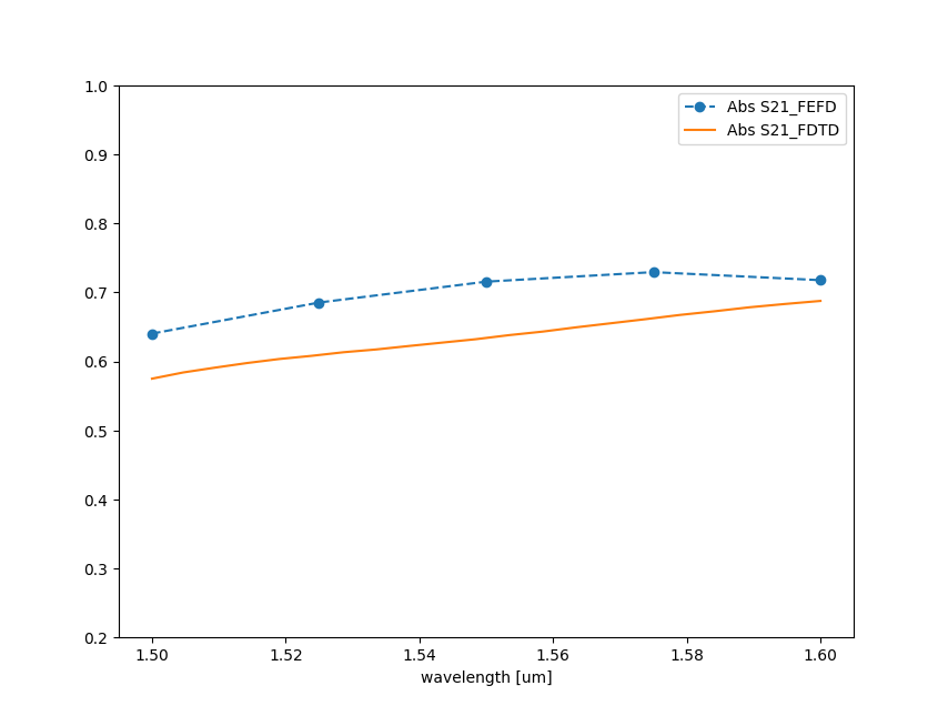
S21
The code also plots the S21 transmission parameter that compared with full 3D simulation should look like.
S31
The code also plots the S31 transmission parameter that compared with full 3D simulation should look like.